Verification Engineer or Senior Verification Engineer SOC at MIPS India

Hello Dear Readers, Currently, at MIPS India  vacancy for a Verification Engineer or Senior Verification Engineer SOC role. We are seeking an experienced Verification Engineer or Senior Verification Engineer SOC. This position involves extensive hands-on experience with CPU verification using industry-standard functional verification methodologies, formal verification, and constrained random generators, and reference model-based checkers. The candidate must be able to take critical decisions and completely own verification closure for a block or feature. This position involves cross-functional interaction with CPU designers and architects and working across sites to ensure high-quality CPU designs for customers. You will: Take full ownership and drive verification efforts to closure Work closely with designers and architects to understand specifications at unit/top level Understand use cases and develop functional test plans Develop directed tests written in C, Assembly, and SystemVeri

ARM Assembly Language Practice Question And Answer Part-2

  Hello Dear Readers, 

Today in this post I will provide some basics to advanced ARM's assembly language practice QA part-2, I have used the Keil tool for code writing.

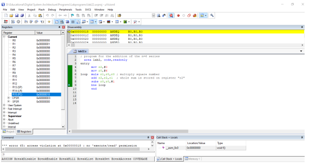
Q-1). Write an assembly language program for storing the sum of first ‘n=6’ terms of the series 1,4,9,16,25…..

Code:

; program for the addition of the n=6 series 

area sum_series, code,readonly 

entry 

mov r2,#0 

mov r0,#6

loop 

  muls r1,r0,r0 ; multiply square number 

  add r2,r2,r1 ; whole sum is stored on register "r2" 

subs r0,r0,#1 

bne loop 

end 

Output:


Q-2). Write an assembly language program to find the maximum of 3 numbers and store it at location 0x5000.

Code:

; program to find maximum number of 3 and store in memory 

area max, code, readonly 

entry 

ldr r0,=data 

ldr r3,=0x5000 

ldr r4,=0x03 ;create a loop of 3 

ldr r1,[r0, #4] 

sub r4,r4,#1 

again 

 ldr r2,[r0] 

 cmp r1,r2 

 bcs loop ; jump on set carry 

 mov r1,r2 

loop 

 add r0,r0,#4 

 sub r4,r4,#1 

 bne again 

str r1,[r3] 

stop b stop 

data dcd 0x07,0x08,0x09 

end 

Output:


Q-3). Write an assembly language program for counting the total occurrences of a given ‘n=3’-bit pattern '110' in a 32-bit value.

Code:

; program to count occurance of the sequences in the given 32 bit value 

area count, code, readonly 

entry 

ldr r0, =data 

mov r3, #0 ; value of the occurance stored 

mov r4, #32 ;defined for one bit calculation 

mov r5, #6 

ldr r1, [r0] 

next 

 mov r1, r1, ror #1 

 mov r2, r1 

 ands r6, r2, r5 ; anding operation for identify sequences 

 subs r6, r6, r5 

 beq again 

 subs r4, r4, #0x1 

 bne next 

 b stop 

again 

 add r3, r3, #0x1 

 subs r4, r4, #0x1 

 bne next 

stop b stop 

data dcd 0x98654353 

end

Output:

Q-4). Write an assembly language program to count the total factors of a number.

Code:

; program to find totals number of factors 

area factor, code, readonly 

entry 

ldr r0,=data 

ldr r1,[r0] ; take example of 4 so number of factor is 3(i.e 1,2,4) 

mov r4,r1 

mov r2,#1 ; initial value for division 

mov r3,#0

next 

 cmp r4,r2 

 bcs loop1 

stop b stop 

loop 

 add r3,r3,#1 

again 

  add r2,r2,#1 

 mov r1,r4 

  b next 

loop1 

subtract 

  SUBS r1,r1,r2 

  beq loop 

  bhi subtract 

 b again 

data dcd 0x04 

end

Output:


Q-5). 
Write an assembly language program to find maximum and minimum values in an array.

Code:

; program to find maximum and minimum value from an array 

area max_min, code, readonly 

entry 

ldr r0,=data 

ldr r1,=0x05 

ldr r3,[r0] ; maximum value stored on r3 register 

ldr r4,[r0] ; minimum value stored on r4 register next 

 ldr r2,[r0] ; it is reference register 

 cmp r3,r2 

 bcs loop 

 mov r3,r2 

loop 

 cmp r4,r2 

 bls again 

 mov r4,r2 

again
  add r0,r0,#4 

  subs r1,r1,#1 

  bne next 

stop b stop 

data dcd 0x03,0x04,0x5,0x7,0x9 

end

Output:


Q-6). 
Write an assembly language program to find the average of first ‘n’ natural numbers.

Code:

; program for calculating average of 'N' natural numbers 

area avg,code,readonly 

entry 

ldr r0,=7 

mov r2,r0 

next 

 add r1,r1,r0 ; addition of all the numbers 7+6+5..... 

 subs r0,r0,#1 

 bne next ; repeat untill addition comes to 0 from the given value 

again 

 sub r1,r1,r2 ; For repeated subtraction 

 add r3,#1 ; r1 is stored remainder 

 cmp r1,r2 ; value in r3 is quotient 

 bge again 

end 

Output:


ARM Assembly Language Practice Question And Answer Part-1


Comments

  1. Wow bro I can't have words for you. Please keep it up to advanced algorithms.

    ReplyDelete

Post a Comment

Popular posts from this blog

SDC (Synopsys Design Constraints) contents part 4

Today, we will be discussing the remaining constraints mentioned in the SDC, which pertain to timing exceptions and design rules. This is the final part of the SDC contents. This is going to be interesting, especially with multicycle paths. Take time to read and try to comprehend. 10. set_max_transition     By setting max transition value, our design checks that all ports and pins are meeting the specified limits mentioned in SDC. If these are not satisfied then timing report will give DRVs (design rule violations) in terms of slack. This is specified as               set_max_transition 0.5  UBUF1/A setting maximum limit of 500ps on pin A of Buffer1. 11. set_max_capacitance     This is same as max transition, setting the maximum capacitance value. if our design not meeting this value then violation will occur. This will also reports under design rule violations in terms of slack.     set_max_capacitance 0.7 [all_nets] setting maximum capacitance of 700fF on all nets. similarly, set_max

Apprenticeship CAI at MediaTek Bangalore

Hello Dear Readers,   Currently at MediaTek Bangalore vacancy for an Apprenticeship CAI role. Job Description: B.Tech degree in Electrical/Electronics Engineering with a strong educational background in Digital circuit design Experience in physical design of high performance design with frequencies > 2 Ghz. Experienced in hierarchical design, budgeting, multiple voltage domains and multiple clock domains. Strong skills with Cadence Encounter. Solid understanding of STA and timing constraints. Experienced in working on advanced process nodes (16nm). Strong expertise in Physical Verification to debug LVS/DRC issues at the block level. Requirement: B.Tech degree in Electrical/Electronics Engineering with strong educational background in Digital circuit design Experience in physical design of high performance design with frequencies > 2 Ghz. Experienced in hierarchical design, budgeting, multiple voltage domains and multiple clock domains. Strong skills with Cadence Encounter. Solid

IC Physical Design (PnR) at Ulkasemi

Hello Dear Readers,   Ulkasemi  has a vacancy for an IC Physical Design (PnR) role. Job Overview: As a full-time Trainee Engineer, the individual will be working on IC Physical Design implementation from RTL to GDSII to create design databases ready for manufacturing with a special focus on power, performance & area optimization with next-generation state-of-the-art process technologies. Job Responsibilities: Perform physical design implementation which includes Floor planning, Power Planning, Clock Tree Synthesis, Place and Route, ECO, Logic Equivalence checks Timing analysis, physical & electrical verification, driving the sign-off closure meeting schedule, and design goals Develop flow, methodologies, and automation scripts for various implementation steps Follow the instructions, compile documents, prepare deliverables, and report to the team lead Should remain up to date with the latest technology trends Educational Qualification:   B.Sc/M.Sc   in EEE or equivalent degree