
Hello Dear Readers, Today in this post, I will provide some deep insight into the VLSI packaging evolution and innovations. Semiconductor packaging has evolved from a simple protective housing into a critical performance enabler. In the modern VLSI landscape, packaging is no longer an afterthought; it is a fundamental determinant of PPA (Power, Performance, and Area) metrics, often dictating the thermal limits and signal integrity of the final SoC. 1. Traditional Packaging Technologies: These methods are the workhorses of the industry, widely used for low-to-medium complexity devices where cost-efficiency is paramount. Wire Bonding (QFN, QFP, DIP): Wire bonding is the most mature interconnection technology. It uses thin gold, copper, or aluminum wires to connect the die's bond pads to the package's internal leadframe. Implementation: The die is attached face-up to a leadframe or substrate. A wire bonder uses thermocompression or ultrasonic energy to attach wires betwee...
Hello Dear Readers,
Today in this post I will provide some basics to advanced ARM's assembly language practice QA I have used the Keil tool for code writing.
Q-1). Perform subtraction of the numbers stored at memory location 0x4000 from the number stored at memory location 0x4004 and place the result in memory location 0x4008.
Code:
; Program of the substraction
area into, code, readonly
entry
mov r1, #0x4000
ldr r2,[r1]
ldr r3,[r1, #4]
sub r4,r3,r2 ; perform substraction operation
str r4,[r1, #8] ; store the result at memory location 0x4008
end
Output:

Q-2). Write a program to check whether the number stored at the memory location is even or odd.
Code:
; program for identity number is even or odd
area prog2, code, readonly
entry
mov r1,#0x4000 ; data location
ldr r2,[r1]
tst r2,#1 ; anding with 0x01 will be updating status
of flag register
bne odd
mov r1,r2 ; even number stored at r1
odd mov r3,r2 ; store odd number
end
Output:

Q-3). Write a program to perform sum of two 64-bit numbers. Use DCD for the same.
Code:
; program of adding two 64 bit data
area sum, code, readonly
entry
ldr r0,=data1
ldr r1,[r0]
ldr r2,[r0,#4]
ldr r0,=data2
ldr r3,[r0]
ldr r4,[r0,#4]
adds r6,r2,r4
adc r5,r1,r3
ldr r0,=result
str r5,[r0]
str r6,[r0,#4]
data1 dcd 0x4000,0x5000
data2 dcd 0x3400,0x2000
result dcd 0
end
Output:

Q-4). Store a number 0xBDA35D12 at location 0x4064. Use DCD for the same.
Code:
; store given data in memory 0x4064
area store, code, readonly
entry
mov r1, #0x4000
ldr r2,=data
ldr r3,[r2]
str r3, [r1, #100]
data dcd 0xBDA35D12
end
Output:

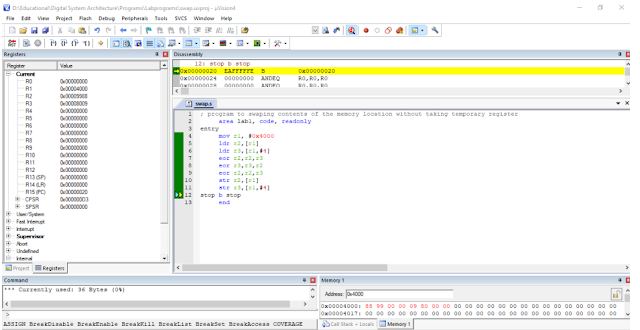
Q-5). Swap the numbers stored at memory locations 0x4000 and 0x4004.
Code:
; program to swaping contents of the memory location without taking temporary register
area swap, code, readonly
entry
mov r1, #0x4000
ldr r2,[r1]
ldr r3,[r1,#4]
eor r2,r2,r3
eor r3,r3,r2
eor r2,r2,r3
str r2,[r1]
str r3,[r1,#4]
stop b stop
end
Output:
Q-6). Write a program to perform the below operations on 0x2020zzFF stored at location 0x4000. Perform the following operations on the number. Store result at memory location 0x4004. a. Selective-clear (on 1st byte) b. Selective-set (on 4th bit) c. Selective-complement (on 2 nd and 3rd byte) d. Selective-set (on 4th byte).
Code:
; program for the desire operation performed on the given data
area selective, code, readonly
entry
mov r1, #0x4000
ldr r2,[r1]
and r2,r2, #0xffffff00
orr r2,r2, #0x00000008
mov r3,#0x0ff00000
mov r4,#0x000f0000
orr r3,r3,r4
eor r2,r2,r3
orr r2,r2, #0xff000000
str r2,[r1, #4]
end
Output:

Now ARM assembly language problem is also solved. Thanks for your effort.
ReplyDeleteWow bro how many parts are you uploading ?
ReplyDeleteNice posts and fabulous examples are there.
ReplyDelete