
Hello Dear Readers, Currently at Global Foundries, vacancy for Senior Eng CAD Engineering role. About GlobalFoundries: GlobalFoundries is a leading full-service semiconductor foundry providing a unique combination of design, development, and fabrication services to some of the world’s most inspired technology companies. With a global manufacturing footprint spanning three continents, GlobalFoundries makes possible the technologies and systems that transform industries and give customers the power to shape their markets. For more information, visit www.gf.com. Introduction: Technology Computer Aided Design tools are critical to accelerate the technology development and deployment in our Fabs. We are seeking to strengthen our TCAD team with highly motivated Individuals who are at the early phase of their career. The candidate brings passion for semiconductor technologies and devices, strives for high-quality work, cares about details, and is willing to learn and cooperate in a...
Hello Dear Readers,
Today in this post I will provide some basics to advanced ARM's assembly language practice QA I have used the Keil tool for code writing.
Q-1). Perform subtraction of the numbers stored at memory location 0x4000 from the number stored at memory location 0x4004 and place the result in memory location 0x4008.
Code:
; Program of the substraction
area into, code, readonly
entry
mov r1, #0x4000
ldr r2,[r1]
ldr r3,[r1, #4]
sub r4,r3,r2 ; perform substraction operation
str r4,[r1, #8] ; store the result at memory location 0x4008
end
Output:

Q-2). Write a program to check whether the number stored at the memory location is even or odd.
Code:
; program for identity number is even or odd
area prog2, code, readonly
entry
mov r1,#0x4000 ; data location
ldr r2,[r1]
tst r2,#1 ; anding with 0x01 will be updating status
of flag register
bne odd
mov r1,r2 ; even number stored at r1
odd mov r3,r2 ; store odd number
end
Output:

Q-3). Write a program to perform sum of two 64-bit numbers. Use DCD for the same.
Code:
; program of adding two 64 bit data
area sum, code, readonly
entry
ldr r0,=data1
ldr r1,[r0]
ldr r2,[r0,#4]
ldr r0,=data2
ldr r3,[r0]
ldr r4,[r0,#4]
adds r6,r2,r4
adc r5,r1,r3
ldr r0,=result
str r5,[r0]
str r6,[r0,#4]
data1 dcd 0x4000,0x5000
data2 dcd 0x3400,0x2000
result dcd 0
end
Output:

Q-4). Store a number 0xBDA35D12 at location 0x4064. Use DCD for the same.
Code:
; store given data in memory 0x4064
area store, code, readonly
entry
mov r1, #0x4000
ldr r2,=data
ldr r3,[r2]
str r3, [r1, #100]
data dcd 0xBDA35D12
end
Output:

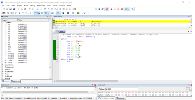
Q-5). Swap the numbers stored at memory locations 0x4000 and 0x4004.
Code:
; program to swaping contents of the memory location without taking temporary register
area swap, code, readonly
entry
mov r1, #0x4000
ldr r2,[r1]
ldr r3,[r1,#4]
eor r2,r2,r3
eor r3,r3,r2
eor r2,r2,r3
str r2,[r1]
str r3,[r1,#4]
stop b stop
end
Output:
Q-6). Write a program to perform the below operations on 0x2020zzFF stored at location 0x4000. Perform the following operations on the number. Store result at memory location 0x4004. a. Selective-clear (on 1st byte) b. Selective-set (on 4th bit) c. Selective-complement (on 2 nd and 3rd byte) d. Selective-set (on 4th byte).
Code:
; program for the desire operation performed on the given data
area selective, code, readonly
entry
mov r1, #0x4000
ldr r2,[r1]
and r2,r2, #0xffffff00
orr r2,r2, #0x00000008
mov r3,#0x0ff00000
mov r4,#0x000f0000
orr r3,r3,r4
eor r2,r2,r3
orr r2,r2, #0xff000000
str r2,[r1, #4]
end
Output:

Now ARM assembly language problem is also solved. Thanks for your effort.
ReplyDeleteWow bro how many parts are you uploading ?
ReplyDeleteNice posts and fabulous examples are there.
ReplyDelete