
Design Engineer - STA, SD, Power, PDN at Dew Software

Hello Dear Readers,   Currently at Dew Software Bangalore vacancy for Design Engineer - STA, SD, Power, PDN role. Dew Software, a leading player in the Digital Transformation space, is seeking a skilled Design Engineer specializing in STA (Static Timing Analysis), SD (Signal Integrity), Power, and PDN (Power Delivery Network) to join our team. Working with Fortune 500 companies to support their digital innovation and transformation strategies, the Design Engineer will be responsible for ensuring the integrity and efficiency of digital designs through comprehensive analysis and optimization. Dew Software is dedicated to delivering exceptional outcomes with cutting-edge technologies, and this is an excellent opportunity to contribute to the growth and success of our clients. Responsibilities: Perform STA (Static Timing Analysis) to ensure design meets timing requirements Conduct signal integrity analysis to optimize signal integrity and minimize signal integrity issues Provide power anal

CMOS Inverter-Layout Design And It functional Verification SPICE Simulation

 Hello Dear Readers,

Today, I will explain how to design a Layout in the MAGIC layout tool and how to perform SPICE simulation.

CMOS inverters (Complementary NMOSFET Inverters) are some of the most widely used and adaptable MOSFET inverters used in chip design. They operate with very little power loss and at relatively high speed. Furthermore, the CMOS inverter has good logic buffer characteristics, in that, its noise margins in both low and high states are large.

A CMOS inverter containing a PMOS and an NMOS transistor connected at the drain and gate terminals, a supply voltage VDD at the PMOS source terminal, and a ground connection at the NMOS source terminal Vin is connected to the gate terminals, and Vout is connected to the drain terminals As shown in Fig.1 is a circuit-level symbol but in the layout-wise internal structure of CMOS is consisted of common P-Type Substrate for building NMOS and N-Well implanted for building PMOS as shown in Fig.2.

                       Fig.1 CMOS Inverter

          Fig.2 CMOS Inverter Internal Structure

So Let's Start the Layout Once You Open the Magic Layout tool Screen is coming as shown in Fig.3. Go to the Window menu and click on "Grid on". So one grid is a square with one lambda by one lambda. So placing layers in magic we need to left-click hold it and right-click where we want to end the shape of the layer. So first I have to build N-well and p-type diffusion overlap as shown in Fig.4 all sizes are optimized by lambda-based design rules.

Fig.3 Magic Layout initial screen

Fig.4 N-well And p-type diffusion overlap

After that now we want to draw a polysilicon layer to build the gate terminal of PMOS. After that metal-1 and substrate contacts layer formed to build complete PMOS as shown in Fig.5. Similarly, we build NMOS and shorted Polysilicon of PMOS and NMOS together to the formed input terminal of the Inverter and shorted the drain layer to the formed output terminal as shown in Fig.6. After that we have to provide labels of VDD, gnd, in, and out as shown in the final layout.  

Fig.5 PMOS

Fig.6 CMOS Inverter final layout

So after the final layout save the layout go to the command line screen of the magic and type first "extract all" and then "ext2spice" as shown in Fig.7. Now go to path in which layout is saved so we found the .spice format file and .mag format file. So copy the .spice file and make a new directory on which paste it and then go to the PTM model and copy the entire web page and make the text file in the same directory on which the spice file was saved. Now open spice file and do some changes such as include model file, apply the supply voltage and input pulse signal for functional verification as shown in Fig.8.


Fig.7 Extract Layout

Fig.8 Updated SPICE file

Now open the terminal from this directory and open Ngspice with spice file as shown in Fig.9 and type command "run" first and then type "plot in out". The simulational waveform is shown in Fig.10.
Spoken Tutorial found Here.


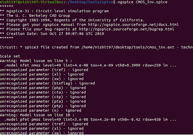
Fig.9 Ngspice simaltion
 
Fig.10 Simulation Waveform of CMOS Inverter


Connect with me 


Comments

  1. Wow first time all doubts regarding Magic plus Ngspice is solved.thanks for your effort

    ReplyDelete
  2. One of the blog in which I found this much easy explanation and project wise learning. Bro keep it up and never stop this work.

    ReplyDelete
  3. Fantastic learning based post.

    ReplyDelete
  4. You are a next level motivation person. Really in india I never find other blog such user friendly.

    ReplyDelete
  5. You are really slow learner, I really like your content accuracy specifically verilog code is always bugs free. So best wish and keep it up

    ReplyDelete
  6. Amazing! Accurate and very well explained.

    ReplyDelete
  7. This comment has been removed by a blog administrator.

    ReplyDelete
  8. Really helpful for beginners

    ReplyDelete
  9. So simple and solved all the query regarding extraction and spice simulation. Thanks dear for your effort 😢😢😢😢

    ReplyDelete
  10. One of the excellent post regarding layout verification through spice simulation. I read your post regularly and big fan of you πŸ‘πŸ‘and I am a professor at IITH.

    ReplyDelete
    Replies
    1. It's my motivation thanks sir for your feedback and appreciation. I will do my best forever.

      Delete
  11. One of superb article

    ReplyDelete
  12. Superb post I really like the way of the contents and simpler explanation.

    ReplyDelete

Post a Comment

Popular posts from this blog

Apprenticeship CAI at MediaTek Bangalore

Hello Dear Readers,   Currently at MediaTek Bangalore vacancy for an Apprenticeship CAI role. Job Description: B.Tech degree in Electrical/Electronics Engineering with a strong educational background in Digital circuit design Experience in physical design of high performance design with frequencies > 2 Ghz. Experienced in hierarchical design, budgeting, multiple voltage domains and multiple clock domains. Strong skills with Cadence Encounter. Solid understanding of STA and timing constraints. Experienced in working on advanced process nodes (16nm). Strong expertise in Physical Verification to debug LVS/DRC issues at the block level. Requirement: B.Tech degree in Electrical/Electronics Engineering with strong educational background in Digital circuit design Experience in physical design of high performance design with frequencies > 2 Ghz. Experienced in hierarchical design, budgeting, multiple voltage domains and multiple clock domains. Strong skills with Cadence Encounter. Solid

Power Analysis in the VLSI Chip Design

  Hello Dear Readers,   Today in this series of posts I will provide some deep insight into Power Analysis in the VLSI Chip Design. The power analysis flow calculates (estimates of) the active and static leakage power dissipation of the SoC design. This electrical analysis step utilizes the detailed extraction model of the block and global SoC layouts. The active power estimates depend on the availability of switching factors for all signals in the cell netlist. Representative simulation test cases are applied to the netlist model, and the signal value change data are recorded. The output data from the power analysis flow guide the following SoC tape out release assessments:  Total SoC power specification (average and standby leakage): The specification for SoC power is critical for package selection and is used by end customers for thermal analysis of the product enclosure. In addition to the package technology selection, the SoC power dissipation is used to evaluate the die attach ma

IC Physical Design (PnR) at Ulkasemi

Hello Dear Readers,   Ulkasemi  has a vacancy for an IC Physical Design (PnR) role. Job Overview: As a full-time Trainee Engineer, the individual will be working on IC Physical Design implementation from RTL to GDSII to create design databases ready for manufacturing with a special focus on power, performance & area optimization with next-generation state-of-the-art process technologies. Job Responsibilities: Perform physical design implementation which includes Floor planning, Power Planning, Clock Tree Synthesis, Place and Route, ECO, Logic Equivalence checks Timing analysis, physical & electrical verification, driving the sign-off closure meeting schedule, and design goals Develop flow, methodologies, and automation scripts for various implementation steps Follow the instructions, compile documents, prepare deliverables, and report to the team lead Should remain up to date with the latest technology trends Educational Qualification:   B.Sc/M.Sc   in EEE or equivalent degree