Today, we will be discussing the remaining constraints mentioned in the SDC, which pertain to timing exceptions and design rules. This is the final part of the SDC contents. This is going to be interesting, especially with multicycle paths. Take time to read and try to comprehend.
10. set_max_transition
By setting max transition value, our design checks that all ports and pins are meeting the specified limits mentioned in SDC. If these are not satisfied then timing report will give DRVs (design rule violations) in terms of slack. This is specified as
set_max_transition 0.5 UBUF1/A
setting maximum limit of 500ps on pin A of Buffer1.
11. set_max_capacitance
This is same as max transition, setting the maximum capacitance value. if our design not meeting this value then violation will occur. This will also reports under design rule violations in terms of slack.
set_max_capacitance 0.7 [all_nets]
setting maximum capacitance of 700fF on all nets.
similarly, set_max_fanout.
The difference between max_capacitance and max_fanout is, max capacitance is maximum allowable load capacitance for each cell or net whereas max fanout is maximum number of loads that each cell/net can drive.
Timing exceptions
12. set_false_path
Certain paths in our design are not real, by setting these paths as false paths we can exclude them from STA analysis. Thus, run time of STA tool will be reduced. The paths which have logically incorrect, the paths whose inputs are tied to either supply or ground called configuration inputs, the paths from test inputs and asynchronous inputs are considered as false paths. These are few examples of false paths but not limited, STA tool cannot identify the false paths as a designer we need to specify.
False path is set using set_false_path. Examples are shown below.
set_false_path -from [get_clocks SCAN_CLK] -to [get_clocks CORE_CLOCK]
set_false_path -through [get_pins UMUX1/A]
Any path passing through multiplexer pin A is ignored for timing analysis.
set_false_path -to [get_ports TEST_REG*]
Any path that ends at the TEST_REG* port are false paths.
Note that "-through" option can slow down the timing analysis so, use it wherever it is absolutely necessary otherwise look for other options to specify such paths.
13. set_multicycle_path
Sometimes data path between launch and capture flop takes more than one clock cycle to propagate the logic, such paths are called multicycle paths (MCP). The normal constraint on this path is overridden to propagate the logic on multiple cycles. For example, setup check for single cycle path is the arrival time at D pin of capture flip flop must be less than the Tclk-Tsu(capture)-Tskew. But it will change for MCP as logic propagated after N clock cycles so setup will be checked at Nth clock cycle then our setup check will be arrival time at D pin of capture flop must be less than N*Tclk-Tsu(capture)-Tskew to capture the data properly. Multicycle path for setup is set by using
create_clock -period 10 [get_ports CLKM]
set_multicycle_path 3 -setup -from [get_pins UFF1/Q] -to [get_pins UFF2/D]
That is setup check will be done at 30ns instead of checking at 10ns.
Similarly, we have to set for hold check. By default hold will check at 1 clock edge before setup check edge (data capture edge). That is if setup check will be done at Nth clock cycle the hold check will be at (N-1)th clock cycle. For this example
set_multicycle_path 2 -hold -from [get_pins UFF1/Q] -to [get_pins UFF2/D].
The actual hold check will be done at 1 cycle before setup that is at 20ns, by setting multiplier 2 it will go backward by 2 cycles. That means hold check will be done at 0ns. If "-hold" option not mentioned then default hold will be checked at 20ns.
Note that setup capture edge moves forward by number of clock cycles specified from the default capture edge whereas hold check edge moves backward by number clock cycles specified from the default hold check edge (that is 1 cycle before setup edge).
Example 1: Let us consider there is a multicycle between two different clock domains with the same period.
create_clock -name CLKM -period 10 [get_ports CLKM]
create_clock -name CLKP -period 10 [get_ports CLKP]
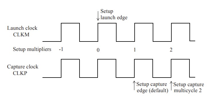
set_multicycle_path 2 -from [get_pins UFF1/Q] -to [get_pins UFF3/D]
Here, no option mentioned so default this is for setup. Note that always checks will be done with respect to capture flop so in timing report path group will always be that of capture flipflop.
In this figure launch edge is at 0 by default capture edge will be 1 cycle away, by setting setup multiplier 2 the capture edge will be put 2 clock cycles away from the launch edge.
If we specify "-hold" option , then
set_multicycle_path 1 -hold -from [get_pins UFF1/Q] -to [get_pins UFF3/D]
Example 2 :Now consider there is multicycle path between two different clock domains with different time period.
create_clock -period 20 [get_ports CLKM]
create_clock -period 5 [get_ports CLKP]
set_multicycle_path 4 -setup -from [get_clocks CLKM] -to [get_clocks CLKP] -end
Here. "-end" indicates the number of capture clock cycles moves by. It is default for multicycle setup. "-start" option indicates the number of launch clock cycles move by. it is default for multicycle hold.
set_multicycle_path 3 -hold -from [get_clocks CLKM] -to [get_clocks CLKP] -end
Here capture edge moved back by 3 clock cycles from default hold check edge. which is shown in below figure.
This post completes the series of SDC contents. In the next post we will discuss more concepts in STA.
Thank you guys for reading the post.


nice article and good explanation
ReplyDelete