
Hello Dear Readers, Today in this post, I will provide some deep insight into the VLSI packaging evolution and innovations. Semiconductor packaging has evolved from a simple protective housing into a critical performance enabler. In the modern VLSI landscape, packaging is no longer an afterthought; it is a fundamental determinant of PPA (Power, Performance, and Area) metrics, often dictating the thermal limits and signal integrity of the final SoC. 1. Traditional Packaging Technologies: These methods are the workhorses of the industry, widely used for low-to-medium complexity devices where cost-efficiency is paramount. Wire Bonding (QFN, QFP, DIP): Wire bonding is the most mature interconnection technology. It uses thin gold, copper, or aluminum wires to connect the die's bond pads to the package's internal leadframe. Implementation: The die is attached face-up to a leadframe or substrate. A wire bonder uses thermocompression or ultrasonic energy to attach wires betwee...
Hello Dear Readers,
Today in this post I will discuss how FPGA is a programmable ASIC and what are the basic building blocks of the FPGA.
Modern FPGAs are named programmable ASICs and used in various applications which include the ASIC SOC designs and prototyping. FPGA programming includes the following types and is discussed below section. The main programming types for any FPGA are,
1). SRAM Based FPGAs:
Most of the FPGAs in the market are based on SRAM technology. They store the configuration bit-file in the SRAM cells designed using latches. As the SRAM is volatile, they need to be configured at the start. There are two modes for programming and they are Master and Slave. The SRAM memory cell is shown in Fig.1. In the Master mode, FPGA reads configuration data from the external source and that can be flash. In the Slave mode, FPGA is configured by using the external master device such as processor. The external configuration interface can be JTAG that is also called as boundary scan.
2). Flash-Based FPGAs:
In this type of FPGAs, flash memory is used to store the configuration data. So the primary resource for this FPGA is flash memory. So these kinds of FPGAs have less power consumption and they are less tolerant of the radiation effects. In the SRAM-based FPGAs, the internal flash is only used during power-up to load the configuration file. The floating gate transistor used in the flash memory is shown in Fig.2.
 |
| Fig. 1: SRAM Cell |
 |
| Fig. 2:Floating gate transistor in flash memory |
3). Antifuse FPGAs:
These types of FPGAs are used to program only once and they are different as compared to the previous two types of FPGAs. Antifuse is opposite to fuse and initially at the start they do not conduct current but can be burned to conduct current. Once they are programmed, there is no any way to reprogram as burned anti-fuse cannot be forced to the initial state. It is shown in Fig.3.
 |
| Fig. 3: Antifuse Structure |
FPGA Basic Buiding Blocks:
The following are key building blocks in the FPGA architecture and are described below section. The FPGA architecture is shown in Fig.4.
I). Configurable Logic Block (CLB):
CLB consists of the Look Up Tables (LUTs), multiplexers, and registers. RAM-based LUTs are used to implement the digital logic. CLBs can be programmed to realize wide variety of logic functions. Even CLBs are used to store the data.
II). Input-Output Block (IOB):
This block is used to control the data flow between the internal logic and IO pins of the device. Each IO is used to support the bidirectional data flow with the tri-state control. There are almost 24 different IO standards which include seven differential special IO high-performance standards. The double data rate registers are also provided with the digital-controlled impedance feature.
III). Block RAM (BRAM):
They are used to store the large amount of the data and available in the form of dual-port RAM. For example 18-Kbit dual-port block RAM. BRAM can consist of such multiple blocks depending on the device.
IV). Digital clock managers (DCMs):
They are used for clock management and provides fully calibrated digital clock solution. They are used for the uniform clock distribution, delay of clock signals, multiply or divide the clock signals with uniform clock skew.
V). Multipliers:
Dedicated multiplier block is used to perform the multiplication of two ‘n’ bit digital numbers. Depending on the device the ‘n’ can vary. If n = 18 then the dedicated block is used to perform the multiplication of two 18-bit numbers.
VI). DSP Blocks:
They are embedded DSP blocks used to realize the DSP functions such as filtering, data processing. These blocks are used to improve the overall performance of the FPGA while processing the huge amount of data for the DSP applications.
 |
| Fig. 4: FPGA architecture (Source Xilinx) |
FPGA Design Flow:
FPGA design flow includes the following key steps and is described in Fig.5.
1. Design entry
2. Design simulation and synthesis
3. Design implementation
4. Device programming.
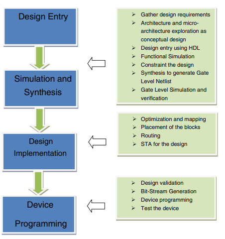 |
| Fig. 5: FPGA design flow |
Thanks For reading and for more details you can search from the below references.
Connect with me
Usefull for interview
ReplyDeleteVery informative thanks for posting
ReplyDeleteI am big fan of your website and you please upload RISC-V synthesized Verilog Code.
ReplyDeleteVery easy explanation as expected
ReplyDeleteSo much easy explanation keep it up
ReplyDeleteFantastic way of explanation
ReplyDeletethanks for posting now I understood complete FPGA internal architectures.
ReplyDelete