
Hello Dear Readers, Today in this post, I will provide some deep insight into the VLSI packaging evolution and innovations. Semiconductor packaging has evolved from a simple protective housing into a critical performance enabler. In the modern VLSI landscape, packaging is no longer an afterthought; it is a fundamental determinant of PPA (Power, Performance, and Area) metrics, often dictating the thermal limits and signal integrity of the final SoC. 1. Traditional Packaging Technologies: These methods are the workhorses of the industry, widely used for low-to-medium complexity devices where cost-efficiency is paramount. Wire Bonding (QFN, QFP, DIP): Wire bonding is the most mature interconnection technology. It uses thin gold, copper, or aluminum wires to connect the die's bond pads to the package's internal leadframe. Implementation: The die is attached face-up to a leadframe or substrate. A wire bonder uses thermocompression or ultrasonic energy to attach wires betwee...
Hello Dear Readers,
Today in this second post we will discuss further standard cells.
A standard cell consists of a set of transistors and their connections which implements a boolean logic or a storage function. Although it is possible to generate any boolean function using only a NAND (or a NOR) gate, the designs will be more area effective by including other logical gates in the library. The elementary gates such as Buffer, Inverter, NAND, NOR, XOR, and memory cells are often found in any standard library while the rich and fancy libraries contain additional gates with higher complexity such as adders and multipliers. The initial design of a standard cell begins with implementing the functionality of the Cell at the transistor level. The schematic view of a cell is used for this purpose. In addition, schematic views are widely used for simulating and debugging circuits. The schematic of a cell can be represented by symbol view which consists of the input and output ports of the cell as well as some text information. Standard cell libraries contain another view which is called layout. Designing the layout view of a cell is compulsory since the netlist is useful for simulation purposes and not for fabrication. The layout of a cell represents what will be physically placed on a chip. Each layout consists of several base layers which form the structures of the transistors and interconnect lines. Designing area-efficient layouts which could meet the required power and timing constraints is still a challenging task despite the existence of different CAD tools to aid the process of design. The designed cell layouts must be checked to ensure that no design rules are violated (Design Rule Check). Then it’s necessary to test the layout by Layout Versus Schematic (LVS) in order to verify the compatibility of the layout with the corresponding schematic. Now, post-layout simulation can be performed by extracting the parasitic after passing the LVS check. The place and route tools need information about the width and height of cells, as well as the location and the dimensions of their input and output pins. The cell layouts are driven to the Abstract Generator, which produces the Library Exchange Format (LEF) file, which contains this information. In addition to the above, LEF files provide information about the technology’s metal stack and the minimum width, spacing, and thickness of the available layers. The layout information of the schematics that we create is available as a GDS file which can be sent for fabrication purposes. GDS (or GDSII) files are usually the final output product of the IC design cycle and are given to IC foundries for IC fabrication.
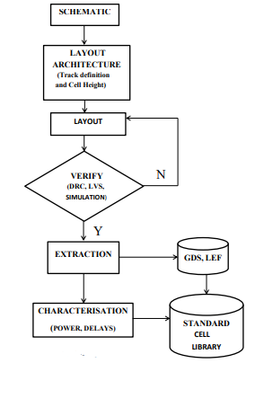 |
| Fig.1 Standard Cell Based Design Flow |
i). STANDARD CELL:
The Standard cells are realized as fixed-height, variable-width full-custom cells, which enable them to be placed in rows, easing the process of automated digital layout. Standard Cells are layouts of logic elements including gates, flip-flops and ALU functions that are available in a cell library for use in a design of a chip. Custom design refers to the design of cells or standard cells using MOSFETs at the lowest level.
The Standard Cell Library can be differentiated into two types: Tapped, Tap less.
A few of the important considerations while designing standard cell architecture are:
1. Pitch
2. DRC
3. Power Rail Width
4. Device Size
5. Tap Cell
6. Pin Accessibility
ii). PITCH:
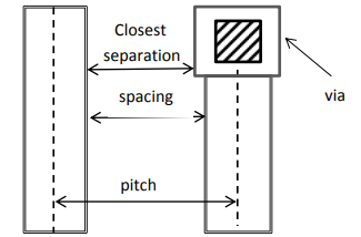
Pitch in the standard cell is the center to center distance of the same metal. Usually, the width is taken as the minimum width of the metal (according to the DRC) so that the area can be kept min. It can be also defined as
Pitch = min width + min spacing
Pitch can be defined in 3 different ways.
1. Line-Line
2. Via-Line
3. Via-Via
Line-Line pitch is the very rarely used architecture. It can be used when the Via size is less than or equal to the min metal width as shown in Fig.2. Otherwise, adjacent tracks cannot be used as placing via causes DRC violation.
 |
| Fig.2 line-to-line pitch |
 |
| Fig.3 line-to-via pitch |
In Via-Via Pitch architecture max number of access points are available. But it consumes more area. In this architecture, every cross-section of horizontal and vertical track can be used as an access point.
 |
| Fig.4 via-to-via pitch |
In the deep submicron process we can also observe that there is a fixed-pitch for poly, which is called a contact to poly pitch (CPP).
iii). DRC:
Design Rules are a series of parameters provided by semiconductor manufacturers that enable the designer to verify the correctness of a mask set. Design rules are specific to a particular semiconductor manufacturing process. A design rule set specifies certain geometric and connectivity restrictions to ensure sufficient margins to account for variability in semiconductor manufacturing processes, so as to ensure that most of the parts work correctly.
 |
| Fig.5 Basics DRC Checks |
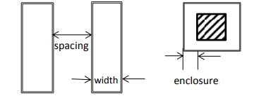
The main objective of design rule checking (DRC) is to achieve a high overall yield and reliability for the design. If design rules are violated the design may not be functional. The most basic design rules are shown in the diagram. The first is single-layer rules. A width rule specifies the minimum width of any shape in the design. A spacing rule specifies the minimum distance between two adjacent objects. These rules will exist for each layer of the semiconductor manufacturing process. A two-layer rule specifies a relationship that must exist between two layers. For example, an enclosure rule might specify that an object of one type, such as a contact or via, must be covered, with some additional margin, by a metal layer. Some examples of DRC’s in IC design include:
1. Active to active spacing
2. Well to well spacing
3. Minimum channel length of the transistor
4. Minimum metal width
5. Metal to metal spacing
During the standard cell design, the designer has to ensure that there is a min of half DRC spacing between cell boundary and layers inside the cell. Good connectivity also should be maintained.
iv). DECIDING POWER RAIL WIDTH :
 |
| Fig.6 N cells placed between common VDD and GND rails |
2. As shown above, due to the resistance offered by the metal there is an IR drop across the length of the metal.
3. Hence even though a voltage of say 1V is applied, (which appears as VDD to Cell 1) the voltage appearing across subsequent cells is less than 1V. This affects the performance of the cell.
4. Hence sufficiently wide VDD rail is necessary so that the cells get sufficient VDD voltage.
5. Normally the maximum tolerable IR drop is about 10% of the applied voltage.
6. To achieve this, we need to choose the appropriate width as the length of the rail is fixed.
7. Consider the following Fig.7, This figure shows two metal1 strips of different widths (w1 and w2). The resistance offered by these is denoted by R1 and R2 respectively. It can be shown that as the width of the strip increases the resistance decreases.(R2 < R1).
 |
| Fig.7 metal strips of widths w1 and w2 |
8. Normally there is no significant IR drop across the length of the metal and we have almost got the applied voltage at the output as well.
v). DEVICE SIZE:
Normally device size is obtained from the schematic. Occasionally device size is negotiable depending on the space available for routing. If the device size is larger, reducing the number of tracks for routing then the fingering technique is used.
vi). TAP CELL:
Standard Cell Library can be designed in 2 ways: With Tap and Without Tap. In with Tap library, each and every cell consists Tap (Substrate connection). This will increase the width of every cell thereby increases the area consumed. It may not necessarily have Taps on each and every cell. Therefore Tap less libraries are created. Here every cell is designed without a Tap and a separated Tap Cell is created. These Tap Cells are placed apart at required distance which reduces the total design area.
E.g.: Consider Width of Inverter with Tap = 2u, Inverter without Tap = 1u, Tap Cell width= 1u, Maximum distance between the Taps= 10u, then We can place 5 Inverters with Tap in 10u space if we use Tapped Library. If we use Tap less library we can place 9 Inverter cells (Without Tap) and a Tap cell in 10u space without violating DRC. In Tapped lib taps can be placed in different positions. Those are Sideways: Taps can place either side of the device. This increases standard cell width.
Top and bottom: Taps can be placed at top and bottom of the device in 3 ways:
1. NWELL tap at the top of P-device and PSUB tap at bottom of N-device.
2. NWELL tap at the top of P-device and PSUB tap at top of N-device.
3. NWELL tap at the bottom of P-device and PSUB tap at bottom of N-device.
vii). PIN ACCESSIBILITY:
Input and output pins should be placed such that they are easily accessible. Pins should be placed at the intersection of horizontal and vertical tracks. This makes placement and routing process easier.
Connect with me
Great information from basics to advanced.
ReplyDeleteUseful starting and how much you will covering through this series.
ReplyDeleteIn the year 2025 I think this website is ideal platform for VLSI contents. Keep it up, I have read every articles.
ReplyDeletePerfect learning site
ReplyDeleteWhen your part-3 coming?
ReplyDeleteVery useful contents keep it up
ReplyDeleteVery beneficial information so whould your part-3 coming or it is ended here?
ReplyDelete