
Hello Dear Readers, Today in this post, I will provide some deep insight into the VLSI packaging evolution and innovations. Semiconductor packaging has evolved from a simple protective housing into a critical performance enabler. In the modern VLSI landscape, packaging is no longer an afterthought; it is a fundamental determinant of PPA (Power, Performance, and Area) metrics, often dictating the thermal limits and signal integrity of the final SoC. 1. Traditional Packaging Technologies: These methods are the workhorses of the industry, widely used for low-to-medium complexity devices where cost-efficiency is paramount. Wire Bonding (QFN, QFP, DIP): Wire bonding is the most mature interconnection technology. It uses thin gold, copper, or aluminum wires to connect the die's bond pads to the package's internal leadframe. Implementation: The die is attached face-up to a leadframe or substrate. A wire bonder uses thermocompression or ultrasonic energy to attach wires betwee...
Hello Dear Readers,
Today, I will explain what are the issues in the mixed-signal circuit layout which is needed to keep in mind while designing the system.
Naturally, analog ICs are more sensitive to noise than digital ICs. For any analog design to be successful, careful attention must be paid to layout issues, particularly in a digital environment. Sensitive analog nodes must be protected and shielded from any potential noise sources. Grounding and power supply routing must also be considered when using digital and analog circuitry on the same substrate. Since a majority of ADCs using switches controlled by digital signals, separate routing channels must be provided for each type of signal.
Techniques used to increase the success of mixed-signal designs vary in complexity and priority. Strategies regarding the systemwide minimization of noise should always be considered foremost. A mixed-signal layout strategy can be modeled as seen in Fig.1. The lowest issues are foundational and must be considered before each succeeding step. The successful mixed-signal design will always minimize the effect of the digital switching on the analog circuits.
 |
| Fig.1 |
The placement of sensitive analog components can greatly affect a circuit's performance. Many issues must be considered. In designing a mixed-signal system, strategies regarding the "floorplan" of the circuitry should be thoroughly analyzed well before the layout is to begin. The analog circuitry should be categorized by the sensitivity of the analog signal to noise. For example, low-level signals or high-impedance nodes typically associated with input signals are considered to be sensitive nodes. These signals should be closely guarded and shielded, especially from digital output buffers. High-swing analog circuits such as comparators and output buffer amplifiers should be placed between the sensitive analog and the digital circuitry. The digital circuitry should also be categorized by speed and function. Obviously, since digital output buffers are usually designed to drive capacitive loads at very high rates, they should be kept farthest from the sensitive analog signals. Next, the high and lower-speed digital should be placed between the insensitive analog and the output buffers. An example of this type of strategy can be seen in Fig.2. Notice that the sensitive analog is as far away as possible from the digital output buffers and that the least sensitive analog circuitry is next to the least offensive digital circuitry.
 |
| Fig.2 |
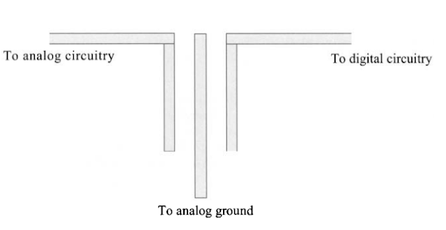
When analog and digital circuits exist together on the same die, the danger exists of injecting noise from the digital system to the sensitive analog circuitry through the power supply and ground connections. Much of the intercoupling can be minimized by carefully considering how power and ground are supplied to both the analog and digital circuits.
3). Guard Rings:
Guard rings should be used wisely throughout a mixed-signal environment. Circuits that process sensory signals should be placed in a separate well (if possible) with guard rings attached to the analog VDD supply. In the case of an n-well (only) process, the n-type devices outside the well should have guard rings attached to analog ground placed around them. Digital circuits should be placed in their own well with guard rings attached to digital VDD. Guard rings placed around the n-channel digital devices also help minimize the amount of noise transmitted from the digital devices.
4). Shielding:
A number of techniques exist which can shield sensitive, low-level analog signals from noise resulting from digital switching. A shield can take the form of a layer tied to analog ground placed between two other layers, or it can be a barrier between two signals running in parallel. If at all possible, one should avoid crossing sensitive analog signals, such as low-level analog input signals, with any digital signals. The parasitic capacitance coupling the two signal lines can be as much as a couple of fF, depending on the process. If it cannot be avoided, then attempt to carry the digital signal using the top layer of metal (such as metal2). If the analog signal is an input signal, then it will most likely be carried by the poly layer (or a lower level of metal). A strip of metal 1 can be placed between the two layers and connected to analog ground as shown in Fig.3.
 |
| Fig.3 |
 |
| Fig.4 |
5). Other Interconnect Considerations:
Finally, some other layout strategies will incrementally improve the performance of the
analog circuitry. However, if the previous strategies are not followed, these suggestions
will be useless. When routing the analog circuitry, minimize the lengths of current-carrying paths. This will simply reduce the amount of voltage drop across the path due to
the metal 1 or metal2 resistance. Vias and contacts should also be used very liberally
whenever changing layers. Not only does this minimize resistance in the path, but it also
improves fabrication reliability. Avoid using poly to route current carrying signal paths.
Not only is the poly higher in resistance value, but also the additional contact resistance
required to change layers will not be insignificant. If the poly is made wider to lower the
resistance, the additional parasitic capacitance will be added to the node. Use poly to route
only high-impedance gate nodes that carry virtually no current.
Connect with me
Comments
Post a Comment