
Hello Dear Readers, Currently at Global Foundries, vacancy for Senior Eng CAD Engineering role. About GlobalFoundries: GlobalFoundries is a leading full-service semiconductor foundry providing a unique combination of design, development, and fabrication services to some of the world’s most inspired technology companies. With a global manufacturing footprint spanning three continents, GlobalFoundries makes possible the technologies and systems that transform industries and give customers the power to shape their markets. For more information, visit www.gf.com. Introduction: Technology Computer Aided Design tools are critical to accelerate the technology development and deployment in our Fabs. We are seeking to strengthen our TCAD team with highly motivated Individuals who are at the early phase of their career. The candidate brings passion for semiconductor technologies and devices, strives for high-quality work, cares about details, and is willing to learn and cooperate in a...
Hello Dear Readers,
Today, I will explain Designing of the different types of counters. There are two types of counter based on the how clock signal is assigned to it namely 1). Synchronous Counters 2). Asynchronous Counter.
1). Synchronous Counters:
If all the storage elements are triggered by the same source clock signal then the design is said to be synchronous. The advantage of the synchronous design is the overall propagation delay for the design is equal to the propagation delay of the flip-flop or storage element. STA is very easy for the synchronous logic and even performance improvement is possible by using the pipelining. Most of the ASIC implementation uses synchronous logic. In practical applications counters are used as a clock divider network. Even counters are used in the frequency synthesizers to generate variable frequency outputs.
i) Parameterized N Bit Up Counter:
Counters are used to generate the predefined and required count sequence on the active edge of the clock. In ASIC design it is essential to write an efficient RTL code for the counter by using the synthesizable constructs. The N-bit-up counter is described by using Verilog to generate the synthesizable design. Here I have design every RTL is parameterized so we can modify it for any number of bits.
Verilog Code:
module counters #(parameter N=3)(data_in,load_en,rst,clk,q_out);
input [N-1:0] data_in;
input load_en,clk,rst;
output reg [N-1:0] q_out;
always@(posedge clk or negedge rst)
begin
if(~rst)
q_out <= 3'b0;
else if(load_en)
q_out <= data_in;
else
q_out <= q_out+1'b1;
end
endmodule
In the above code, the procedural block is sensitive to the clock(clk) and reset(rst) signal. Here for reset 'rst=0' is assign 3'b000 to the q_out. So it is called asynchronous reset and it has the highest priority over any other input. Similarly, if you want to design a down counter as shown below.
Verilog Code:
module counters #(parameter N=3)(data_in,load_en,rst,clk,q_out);
input [N-1:0] data_in;
input load_en,clk,rst;
output reg [N-1:0] q_out;
always@(posedge clk or negedge rst)
begin
if(~rst)
q_out <= 3'b0;
else if(load_en)
q_out <= data_in;
else
q_out <= q_out-1'b1;
end
endmodule
Now if we want to design a Common Up-Down counter based on signal value let's say one-bit 'up_down' signal if its value '1' counter work as an up counter and if the value is '0' then it works as a down counter. Synthesized RTL Verilog is shown below.
Verilog Code:
module counters #(parameter N=3)(data_in,load_en,rst,clk,up_down,q_out);
input [N-1:0] data_in;
input load_en,clk,rst,up_down;
output reg [N-1:0] q_out;
always@(posedge clk or negedge rst)
begin
if(~rst)
q_out <= 3'b0;
else if(load_en)
q_out <= data_in;
else
begin
if(up_down)
q_out <= q_out+1'b1;
else
q_out <= q_out-1'b1;
end
end
endmodule
(ii) Gray Counters:
Gray Counters is another example of a synchronous counter. Gray counters are used in the multiple clock domain designs as only one-bit changes on the active clock edge. Gray codes are used in the synchronizers. The Gray counter is described below. In which first we increment input data as binary counter and then using code converter algorithms final output is Gray counter which is represented by 'q_out'.
Verilog Code:
module counters #(parameter N=4)(data_in,load_en,rst,clk,up_down,q_out);
input [N-1:0] data_in;
input load_en,clk,rst,up_down;
output reg [N-1:0] q_out;
reg q2,q1,q0;
reg [N-1:0] count;
always@(posedge clk)
begin
if(rst) begin
q_out <= 4'b0;
{q2,q1,q0}<=3'b0;
count<=4'b0;
q_out<=4'b0;
end
else if(load_en) begin
count <= data_in;
{q2,q1,q0}<={data_in[2],data_in[1],data_in[0]};
q_out<={data_in[3],data_in[2],data_in[1],data_in[0]};
end
else
begin
count<= count+1'b1;
q2<=count[3]^count[2];
q1<=count[2]^count[1];
q0<=count[1]^count[0];
q_out<={count[3],q2,q1,q0};
end
end
endmodule
(iii) Ring Counters:
Ring Counters is a synchronous counter where the sequence is repeated after few clock cycles. Ring Counters are used in practical applications to provide the predefined delay. These counters are synchronous in nature and used in practical applications like traffic light controller, timers to introduce the certain amount of predefined delay. The internal logic structure using the D flip-flops for the four-bit ring counter is shown in Fig.1, as shown the output of MSB flip-flop is fed back to the LSB flip-flop input, and the counter shifts the data on every active edge of clock signal.
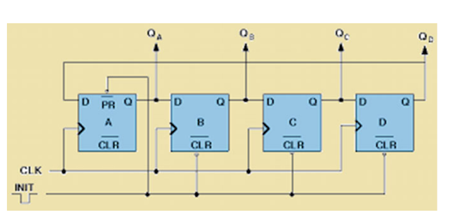 |
| Fig. 1 |
Verilog Code:
module counters #(parameter N=4)(set_in,clk,q_out);
input set_in;
input clk;
output reg [N-1:0] q_out;
always@(posedge clk)
if(set_in)
begin
q_out<=4'b1000;
end
else
begin
q_out<=q_out<<1; // describe functionality that MSB is feedback to the LSB
q_out[0]<=q_out[3];
end
end
endmodule
(iv) Johnson Counters:
Johnson Counter is a special type of synchronous counter and designed by using the shift register. The internal structure for the three-bit Johnson counter is shown in Fig.2. The Verilog RTL for the four-bit Johnson counter is shown below.
 |
| Fig.2 |
Verilog Code:
module counters #(parameter N=4)(rst,clk,q_out);
input rst;
input clk;
output reg [N-1:0] q_out;
always@(posedge clk or negedge rst)
begin
if(~rst)
q_out<=4'b0;
else
q_out<={{q_out[2:0]},{~q_out[3]}};
end
endmodule
2). Asynchronous Counters:
In the asynchronous counters, the clock signal is not driven by the common clock source. If the output of the LSB flip-flop is given as an input to the subsequent flip-flop then the design is asynchronous. The issue with the asynchronous design is the cumulative clock to q delay of flip-flop due to the cascading of the stages. Asynchronous counters are not recommended in the ASIC design due to the issue of glitches or spikes and even the timing analysis for such kind of design is very complex.
Ripple Counters:
The ripple counter is an asynchronous counter and is shown in Fig.3. As shown in the logic diagram all the flip-flops are positive edge triggered and the LSB register receives the clock from the master clock source. The output of the LSB flip-flop is given as clock input to the next subsequent stage.
 |
| Fig.3 |
The Verilog RTL for the four-bit ripple up counter is shown below.
Verilog Code:
module ripple_counters #(parameter N=4)(rst,clk,togle_in,q_out);
input rst,clk,togle_in;
output reg [N-1:0] count_out;
wire c0,c1,c2;
assign c0=count_out[0];
assign c1=count_out[1];
assign c2=count_out[2];
always@(posedge clk or negedge rst)
begin
if(~rst)
count_out[0]<=1'b0;
else if(togle_in)
count_out[0]<=~count_out[0];
always@(negedge rst or negedge c0)
begin
if(~rst)
count_out[1]<=1'b0;
else if(togle_in)
count_out[1]<=~count_out[1];
always@(negedge rst or negedge c1)
begin
if(~rst)
count_out[2]<=1'b0;
else if(togle_in)
count_out[2]<=~count_out[2];
always@(negedge rst or negedge c2)
begin
if(~rst)
count_out[3]<=1'b0;
else if(togle_in)
count_out[3]<=~count_out[3];
endmodule
Thanks for reading and comment your doubts I will try to resolve early as possible.
Connect with me
Wow bro really helpful post.
ReplyDeleteWonderful post bro keep it up
ReplyDeleteSuperb flow of information.
ReplyDelete