
Hello Dear Readers, Today in this post, I will provide some deep insight into the VLSI packaging evolution and innovations. Semiconductor packaging has evolved from a simple protective housing into a critical performance enabler. In the modern VLSI landscape, packaging is no longer an afterthought; it is a fundamental determinant of PPA (Power, Performance, and Area) metrics, often dictating the thermal limits and signal integrity of the final SoC. 1. Traditional Packaging Technologies: These methods are the workhorses of the industry, widely used for low-to-medium complexity devices where cost-efficiency is paramount. Wire Bonding (QFN, QFP, DIP): Wire bonding is the most mature interconnection technology. It uses thin gold, copper, or aluminum wires to connect the die's bond pads to the package's internal leadframe. Implementation: The die is attached face-up to a leadframe or substrate. A wire bonder uses thermocompression or ultrasonic energy to attach wires betwee...
Hello Dear Readers,
Today In this post I have implemented Restoring Division Algorithm Using Verilog HDL. So I have followed this One video from Tutorial Point Youtube Channel So go through it before Verilog code.
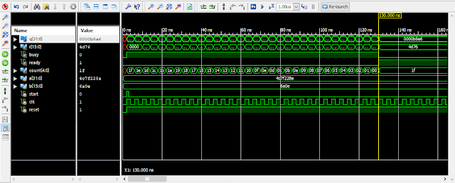
start means the start of the division; busy indicates that the divider is busy (cannot start a new division); ready indicates that the quotient and remainder are available, and the count is the output of a counter that is used to control the iterations of the division.
Verilog Code(Restoring):
module divider_32(a,b,start,clk,reset,q,r,busy,ready,count);
input [31:0] a; // dividend
input [15:0] b; // divisor
input start; // start
input clk,reset; // clk,reset
output [31:0] q; // quotient
output [15:0] r; // remainder
output reg busy; // busy
output reg ready; // ready
output [4:0] count; // counter
reg [31:0] reg_q;
reg [15:0] reg_r;
reg [15:0] reg_b;
reg [4:0] count;
wire [16:0] sub_out = {reg_r,reg_q[31]} - {1'b0,reg_b}; // sub
wire [15:0] mux_out = sub_out[16]? // restoring logic
{reg_r[14:0],reg_q[31]} : sub_out[15:0]; // or not
assign q = reg_q;
assign r = reg_r;
always @ (posedge clk or negedge reset) begin
if (!reset) begin
busy <= 0;
ready <= 0;
end else begin
if (start) begin
reg_q <= a; // load a
reg_b <= b; // load b
reg_r <= 0;
busy <= 1;
ready <= 0;
count <= 31;
end else if (busy) begin
reg_q <= {reg_q[30:0],~sub_out[16]}; // << 1
reg_r <= mux_out;
count <= count - 5'b1; // counter++
if (count == 5'h0) begin // finished
busy <= 0;
ready <= 1; // q,r ready
end
end
end
end
endmodule
Verilog Code(Non Restoring):
module nonrestore_32(a,b,start,clk,reset,q,r,busy,ready,count);
input [31:0] a; // dividend
input [15:0] b; // divisor
input start; // start
input clk,reset; // clk,reset
output [31:0] q; // quotient
output [15:0] r; // remainder
output reg busy; // busy
output reg ready; // ready
output [4:0] count; // count
reg [31:0] reg_q;
reg [15:0] reg_r;
reg [15:0] reg_b;
reg [4:0] count;
wire [16:0] sub_add = reg_r[15]?
{reg_r,reg_q[31]} + {1'b0,reg_b} : // + b
{reg_r,reg_q[31]} - {1'b0,reg_b}; // - b
assign q = reg_q;
assign r = reg_r[15]? reg_r + reg_b : reg_r; // adjust r
always @ (posedge clk or negedge reset) begin
if (!reset) begin
busy <= 0;
ready <= 0;
end
else begin
if (start) begin
reg_q <= a; // load a
reg_b <= b; // load b
reg_r <= 0;
busy <= 1;
ready <= 0;
count <= 0;
end else if (busy) begin
reg_q <= {reg_q[30:0],~sub_add[16]}; // << 1
reg_r <= sub_add[15:0];
count <= count + 5'b1; // count++
if (count == 5'h1f) begin // finish
busy <= 0;
ready <= 1; // q,r ready
end
end
end
end
endmodule
Testbench:
module tb();
reg [31:0] a; // dividend
reg [15:0] b; // divisor
reg start; // start
reg clk,reset; // clk,reset
wire [31:0] q; // quotient
wire [15:0] r; // remainder
wire busy; // busy
wire ready; // ready
wire [4:0] count; // counter
//Device Under Test(DUT)
divider_32 test(a,b,start,clk,reset,q,r,busy,ready,count);
always
#2 clk=~clk;
initial begin
reset=0;
clk=0;
start=0;
a=32'h4c7f228a;
b=32'h6a0e;
#2
reset=1;
start=1;
#1
start=0;
end
endmodule
Timing Parameters:
Minimum period: 5.325ns (Maximum Frequency: 187.786MHz)
Minimum input arrival time before clock: 4.389ns
Maximum output required time after clock: 4.252ns
Thanks for your effort for giving test bench also and you are only one who provide complete expected code.
ReplyDeleteThanks for appreciation
DeleteGreat post ☺️
ReplyDeleteWow Non restore also added
ReplyDelete