
Hello Dear Readers, Today in this post, I will provide some deep insight into the VLSI packaging evolution and innovations. Semiconductor packaging has evolved from a simple protective housing into a critical performance enabler. In the modern VLSI landscape, packaging is no longer an afterthought; it is a fundamental determinant of PPA (Power, Performance, and Area) metrics, often dictating the thermal limits and signal integrity of the final SoC. 1. Traditional Packaging Technologies: These methods are the workhorses of the industry, widely used for low-to-medium complexity devices where cost-efficiency is paramount. Wire Bonding (QFN, QFP, DIP): Wire bonding is the most mature interconnection technology. It uses thin gold, copper, or aluminum wires to connect the die's bond pads to the package's internal leadframe. Implementation: The die is attached face-up to a leadframe or substrate. A wire bonder uses thermocompression or ultrasonic energy to attach wires betwee...
Hello Dear Readers,
Here I have designed a 4 tap FIR filter using Verilog languages and some parts of the Python language to just print the input and output samples that are generating Verilog HDL.
So Let's see the Code of the complete system.
So first of all FIR filter is a system which transfer function has a finite number of impulsive points corresponding to the type of the filters such as high pass, low pass, bandpass, etc... so it has generally two types of structure as shown in the below,
FIR Filter Structures:


Here I have used the first structure in which first multiply input samples with impulse responses so without delay products is available now we give delays to that data means here we have implemented shifted adder for MAC operation of the digital filter.
Verilog Code:
module fir_4tap(input Clk,input signed [7:0] Xin,output reg signed [15:0] Yout);
//Internal variables.
wire signed [7:0] H0,H1,H2,H3;
wire signed [15:0] MCM_block0,MCM_block1,MCM_block2,MCM_block3,shift_add_out1,shift_add_out2,shift_add_out3,Q1,Q2,Q3;
//filter coefficient initializations.
//h(n) = [-1 -2 5 -1].
assign H0 = -1;
assign H1 = -2;
assign H2 = 5;
assign H3 = -1;
//Multiple constant multiplications.
assign MCM_block3 = H3*Xin;
assign MCM_block2 = H2*Xin;
assign MCM_block1 = H1*Xin;
assign MCM_block0 = H0*Xin;
//adders
assign shift_add_out1 = Q1 + MCM_block2;
assign shift_add_out2 = Q2 + MCM_block1;
assign shift_add_out3 = Q3 + MCM_block0;
//flipflop instantiations (for introducing a delay).
DFF dff1 (.Clk(Clk),.D(MCM_block3),.Q(Q1));
DFF dff2 (.Clk(Clk),.D(shift_add_out1),.Q(Q2));
DFF dff3 (.Clk(Clk),.D(shift_add_out2),.Q(Q3));
//Assign the last adder output to final output.
always@ (posedge Clk)
Yout <= shift_add_out3;
endmodule
module DFF(input Clk,input [15:0] D,output reg [15:0] Q);
always@ (posedge Clk)
Q = D;
endmodule
module test_bench;
// Inputs
reg Clk;
reg signed [7:0] Xin ;
// Outputs
wire signed [15:0] Yout;
integer outfile1,outfile2;
// Instantiate the Unit Under Test (UUT)
fir_4tap uut (
.Clk(Clk),
.Xin(Xin),
.Yout(Yout)
);
//Generate a clock with 10 ns clock period.
initial Clk = 0;
always
#5 Clk =~Clk;
//Initialize and apply the inputs.
initial begin
Xin =0; #40;
outfile1=$fopen("output.txt","w");
outfile2=$fopen("input.txt","w");
$fwrite(outfile1,"%d\n",Xin); //write as decimal
$fwrite(outfile2,"%d\n",Yout); //write as decimal
Xin =0.5; #10;
$fwrite(outfile1,"%d\n",Xin); //write as decimal
$fwrite(outfile2,"%d\n",Yout); //write as decimal
Xin =1; #10;
$fwrite(outfile1,"%d\n",Xin); //write as decimal
$fwrite(outfile2,"%d\n",Yout); //write as decimal
Xin =1.5; #10;
$fwrite(outfile1,"%d\n",Xin); //write as decimal
$fwrite(outfile2,"%d\n",Yout); //write as decimal
Xin =2; #10;
$fwrite(outfile1,"%d\n",Xin); //write as decimal
$fwrite(outfile2,"%d\n",Yout); //write as decimal
Xin =1.6; #10;
$fwrite(outfile1,"%d\n",Xin); //write as decimal
$fwrite(outfile2,"%d\n",Yout); //write as decimal
Xin =0.8; #10;
$fwrite(outfile1,"%d\n",Xin); //write as decimal
$fwrite(outfile2,"%d\n",Yout); //write as decimal
Xin =0.5; #10;
$fwrite(outfile1,"%d\n",Xin); //write as decimal
$fwrite(outfile2,"%d\n",Yout); //write as decimal
Xin =0; #10;
$fwrite(outfile1,"%d\n",Xin); //write as decimal
$fwrite(outfile2,"%d\n",Yout); //write as decimal
Xin =-0.5; #10;
$fwrite(outfile1,"%d\n",Xin); //write as decimal
$fwrite(outfile2,"%d\n",Yout); //write as decimal
Xin =-1; #10;
$fwrite(outfile1,"%d\n",Xin); //write as decimal
$fwrite(outfile2,"%d\n",Yout); //write as decimal
Xin =-1.2; #10;
$fwrite(outfile1,"%d\n",Xin); //write as decimal
$fwrite(outfile2,"%d\n",Yout); //write as decimal
Xin =-2; #10;
$fwrite(outfile1,"%d\n",Xin); //write as decimal
$fwrite(outfile2,"%d\n",Yout); //write as decimal
Xin =-1.7; #10;
$fwrite(outfile1,"%d\n",Xin); //write as decimal
$fwrite(outfile2,"%d\n",Yout); //write as decimal
Xin =-1.2; #10;
$fwrite(outfile1,"%d\n",Xin); //write as decimal
$fwrite(outfile2,"%d\n",Yout); //write as decimal
Xin =-0.8; #10;
$fwrite(outfile1,"%d\n",Xin); //write as decimal
$fwrite(outfile2,"%d\n",Yout); //write as decimal
Xin =-0.4; #10;
$fwrite(outfile1,"%d\n",Xin); //write as decimal
$fwrite(outfile2,"%d\n",Yout); //write as decimal
Xin =0; #10;
$fwrite(outfile1,"%d\n",Xin); //write as decimal
$fwrite(outfile2,"%d\n",Yout); //write as decimal
$fclose(outfile1);
$fclose(outfile2);
end
endmodule
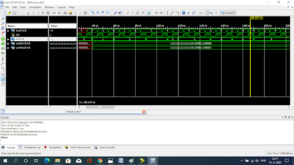
Simulational Results:
Summary of the Obtained Timing Specification:
Timing Specification:
1.Minimum period: 3.644ns (Maximum Frequency: 274.424MHz)
2. Minimum input arrival time before clock: 9.081ns (Setup Time)
3. Maximum output required time after clock: 4.040ns (Hold Time)
Great post you are first person who is this much technically writing blogging keep it up.
ReplyDeleteThanks for reading it is my pleasure.
Deletewhat a post brother thanks for posting i have try it and change according to my requirement.
ReplyDeleteIt is in complete level of the data path means RTL Verilog code right? what we do for the gate level code.
ReplyDeleteSo you need to design adder and multiplier at gate level and then instant them in your main code where addition and multiplication is required.
Delete